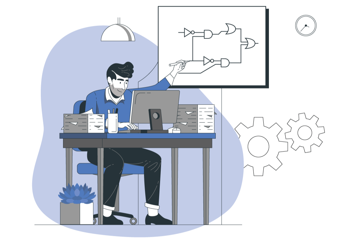
Your one stop RTL-to-GDSII solution!
Your complete RTL-to-GDSII solution, delivering efficiency and expertise at every step of the process. Trust us to bring your semiconductor designs to life seamlessly and successfully.
Your complete RTL-to-GDSII solution, delivering efficiency and expertise at every step of the process. Trust us to bring your semiconductor designs to life seamlessly and successfully.
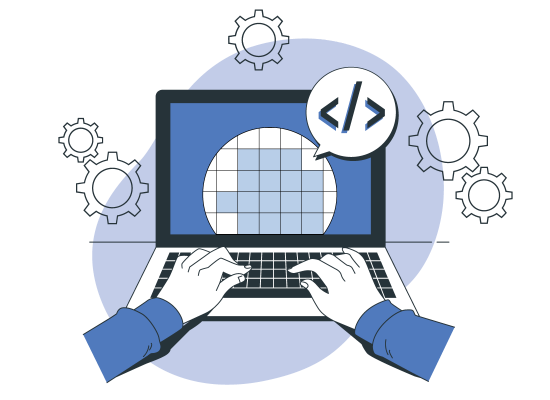
 Integrate
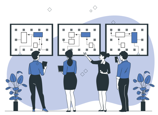
 Turn-Key
Solution
Turn-Key
Solution
 PDK & Library Evaluation
 Synthesis
 DFT and ATPG
 Formal Verification
 Place and Route
 Physical Verification
 Timing Closure
 Power/IR Analysis
 Post-Silicon ECO